The complete guide to PCB pad :types, size, spacing, repair and comparison - IBE Electronics

Soldering is one of the most important processes in PCBA processing. On printed circuit boards, electrical connections to all components are made via PCB pads. The PCB pads are a very critical part of the PCB that determines where components are soldered on the PCB.The size, shape, and position of pads in a PCB directly depend on the manufacturing quality of the board. Today we will take a look at the PCB pad in SMT soldering.
Soldering is one of the most important processes in PCBA processing. On printed circuit boards, electrical connections to all components are made via PCB pad.

Via-in-Pad - PCB Prototype the Easy Way - PCBWay

Ultimate Guide to PCB Layout Design Considerations

PCB Pads shape and size design standards
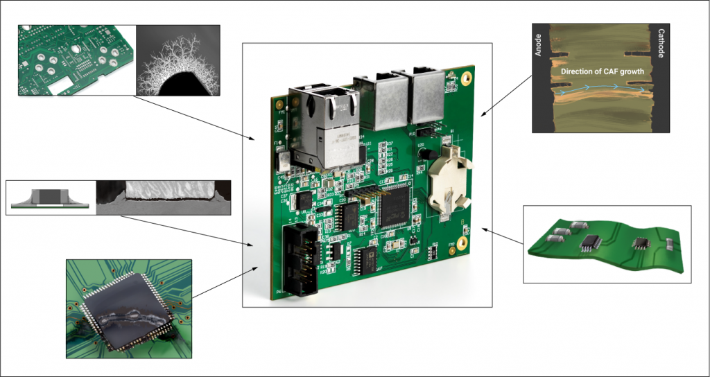
Types of Electronic Component Failures in PCBs

The complete guide to PCB pad :types, size, spacing, repair and comparison - IBE Electronics

Best Methods for Calculating SMD Pad Size in PCB Design
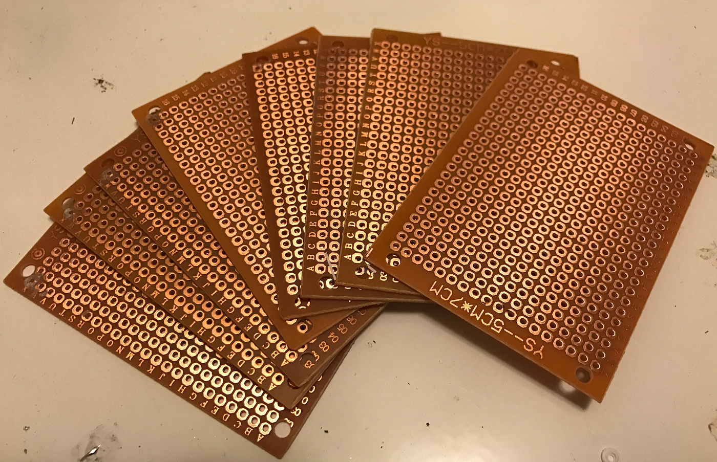
Notes on prototyping circuit boards: breadboards, perfboards, and beyond, by R. X. Seger

Xiaomi Packs 48-megapixel Camera Into Budget Redmi Note, 55% OFF
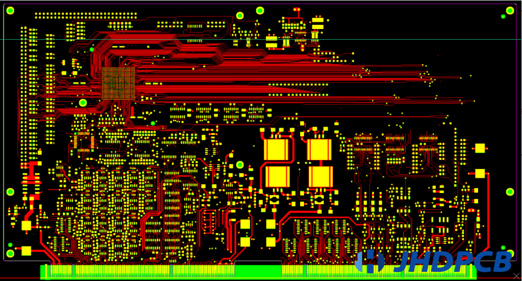
Complete Guide To PCB Layout Design Steps And Rules - Jhdpcb