Details of test chip designs: pad pitch, layout, materials, and opening.
![](https://www.researchgate.net/profile/Paul-Conway-9/publication/28578026/figure/fig1/AS:670717242773506@1536922860459/Details-of-test-chip-designs-pad-pitch-layout-materials-and-opening_Q320.jpg)
![](https://upload.wikimedia.org/wikipedia/commons/8/8a/Solder_ball_grid.jpg)
Ball grid array - Wikipedia
![](https://www.researchgate.net/publication/4292767/figure/fig4/AS:646779825565698@1531215735315/The-layout-of-a-test-chip.png)
The layout of a test chip. Download Scientific Diagram
![](https://www5.cadence.com/rs/070-BII-206/images/e2e_banner.jpg)
Top PCB Layout Recommendations for BGA Packages
![](https://www.researchgate.net/profile/Friedrich-Leonhard-Schein/publication/337584117/figure/fig2/AS:830075746406401@1574916888199/Package-and-chip-design.png)
Package and chip design. Download Scientific Diagram
![](https://pub.mdpi-res.com/jlpea/jlpea-11-00002/article_deploy/html/images/jlpea-11-00002-g001.png?1610067416)
pub.mdpi-res.com/jlpea/jlpea-11-00002/article_depl
![](https://media.springernature.com/full/springer-static/image/art%3A10.1038%2Fs41928-024-01126-y/MediaObjects/41928_2024_1126_Fig1_HTML.png)
High-performance, power-efficient three-dimensional system-in-package designs with universal chiplet interconnect express
![](https://images.surferseo.art/17caf69f-40c4-4be5-84d4-310efe689959.png)
PCB Assembly: Printed Circuit Board Assembly (PCBA) Process
![](https://jhdpcb.com/wp-content/uploads/2022/08/BGA-example2.webp)
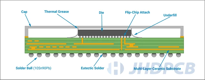
IC PCB Package Type: Importance And Guidelines - Jhdpcb
![](https://media.springernature.com/full/springer-static/image/art%3A10.1038%2Fs41586-023-06337-5/MediaObjects/41586_2023_6337_Fig1_HTML.png)
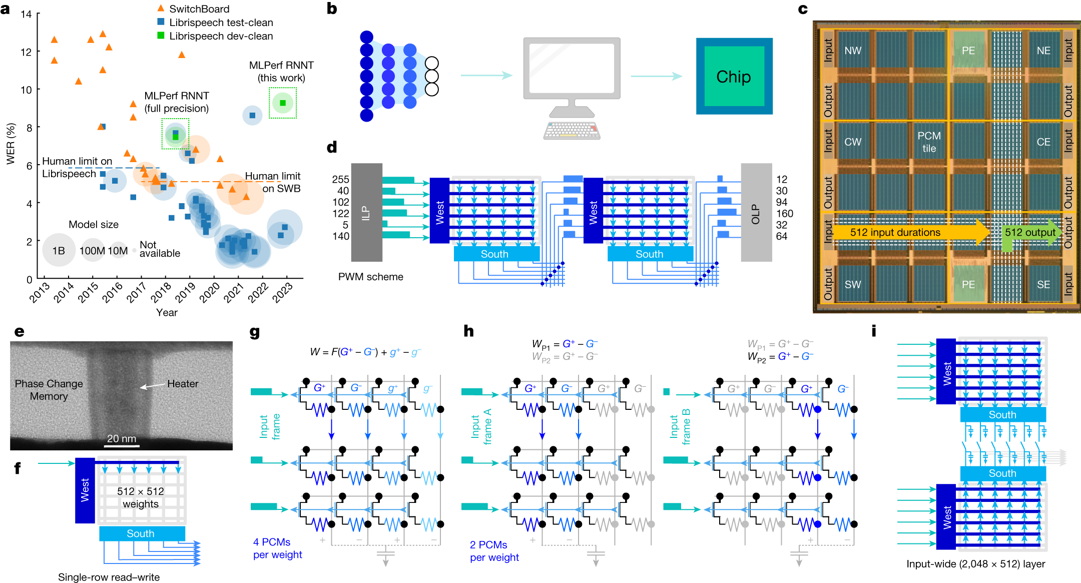
An analog-AI chip for energy-efficient speech recognition and transcription
![](https://d3i71xaburhd42.cloudfront.net/fb1de5a4f5fca2689d82a8529a640346521e051b/2-Table1-1.png)
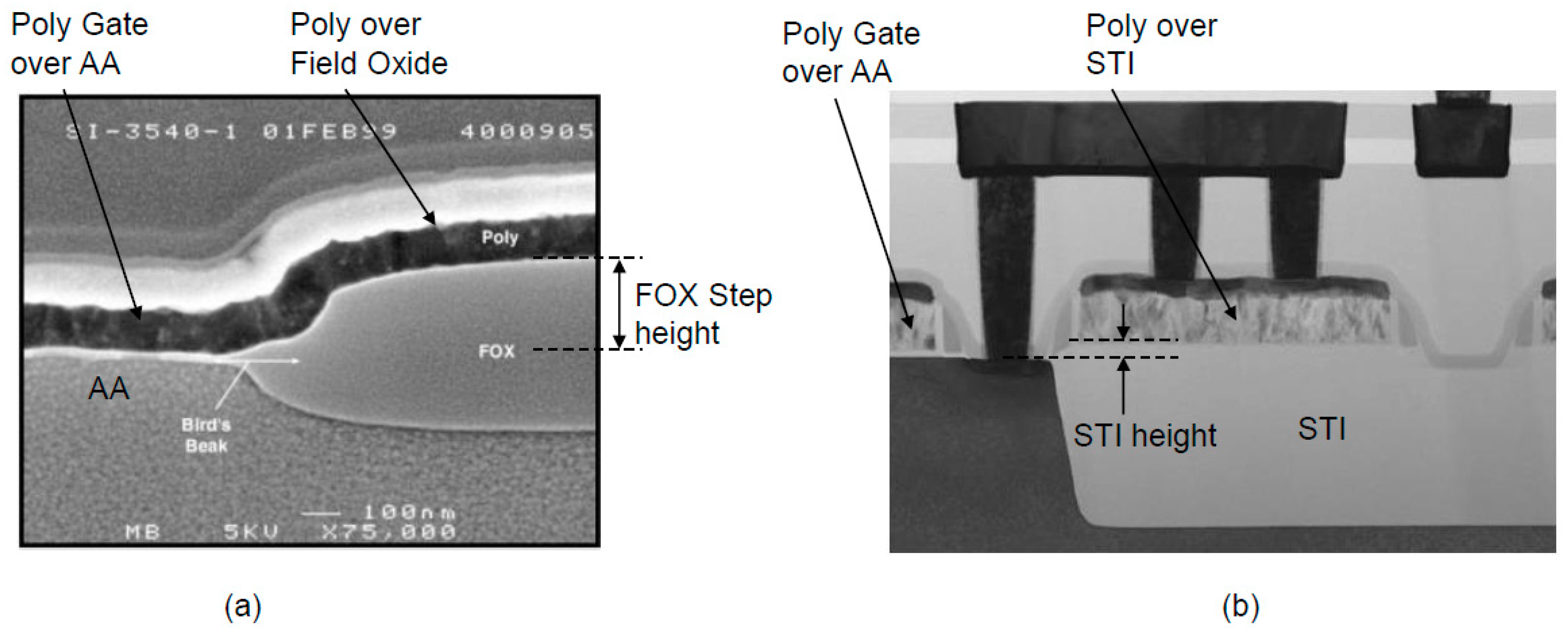
Design and characterization of a copper-pillar flip chip test vehicle for small form-factor packages using 28nm ELK die and bump-on-trace (BOT)