PCB Via Size and Pad Size Guidelines, Zach Peterson
Do you know what PCB via size you should use in your PCB layout? We’ll look at a few simple ways to answer this question.

US9465412B2 - Input device layers and nesting - Google Patents
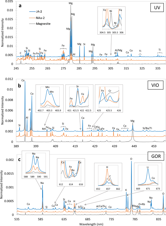
The SuperCam Instrument Suite on the NASA Mars 2020 Rover: Body Unit and Combined System Tests

Anjali Deshpande- Kulkarni on LinkedIn: #pcbdesign #pcblayout

PCB Via Size and Pad Size Guidelines, Zach Peterson, Blog

We have all been there… 😅🤚 I promise it gets better 👍 #pcbdesign #l

Md Ammar Maniyar on LinkedIn: #555timer #pwmmotorcontroller #easyeda #circuitdesign #diyelectronics…

A cell-type-specific atlas of the inner ear transcriptional response to acoustic trauma - ScienceDirect

PCB Via Size and Pad Size Guidelines, Zach Peterson, Blog

US9411751B2 - Key formation - Google Patents