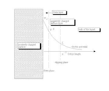
10. Schematic illustration of electrical double layer structure

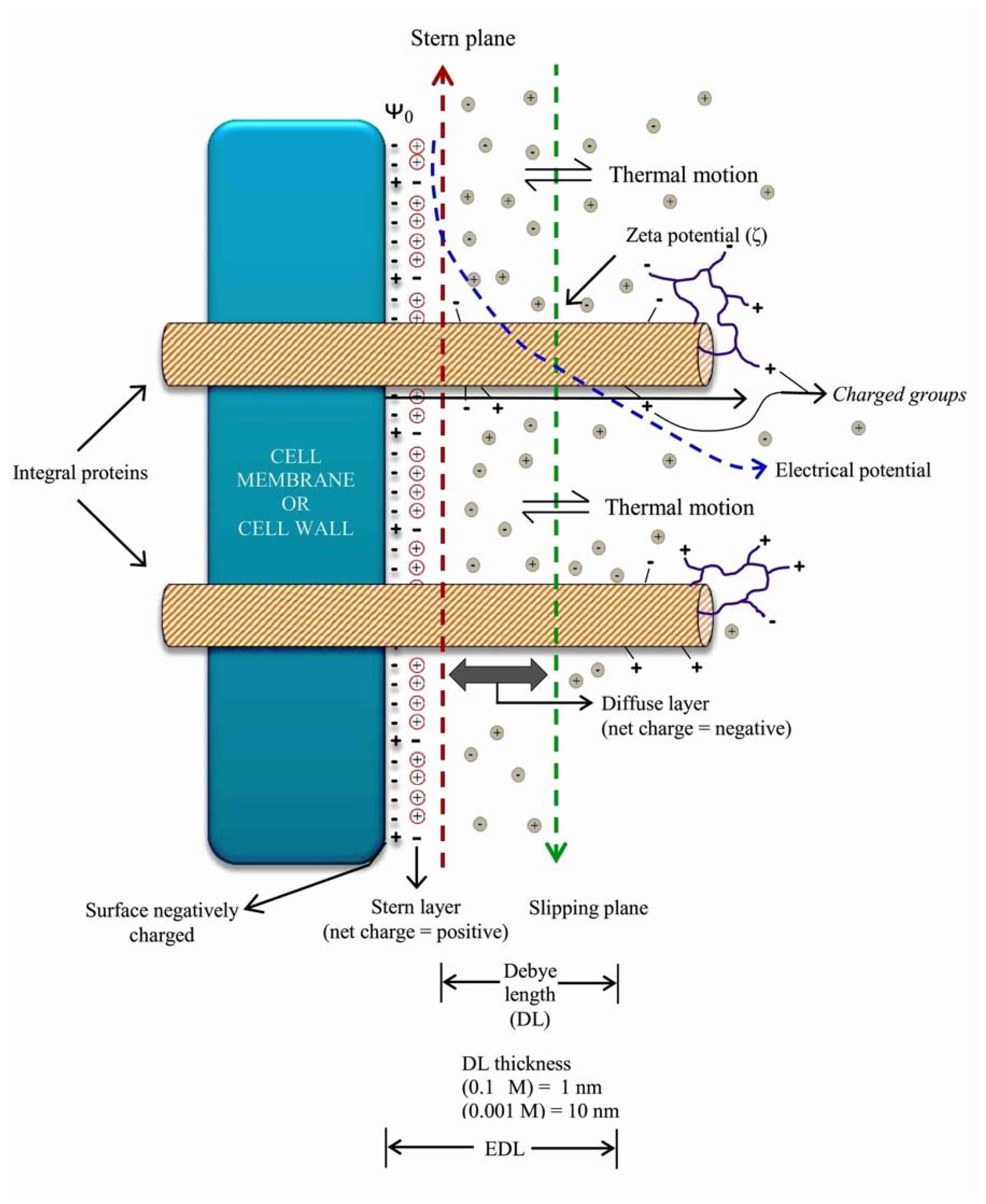
Download scientific diagram | 10. Schematic illustration of electrical double layer structure and the electric potential close to a solid surface with a stern and diffuse layer. Reproduced with permission from Elsevier from ref. [90]. from publication: Development and characterization of new bioactive and antibacterial coatings for biomedical applications using electric field assisted processing | The stability of implants and their long-term survival requires early anchorage at the bone implant interface. This early osteointegration process requires the recruitment of different cells on the periprosthetic site. There is evidence suggesting that a lack of | Zein, Coatings and Antibacterials | ResearchGate, the professional network for scientists.
How to Draw and Design a PCB Schematic
Energies, Free Full-Text

Particle Dispersion for Size Analysis - Particle Technology Labs
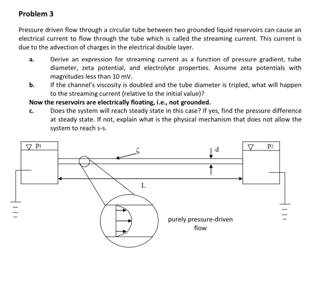
Solved Pressure driven flow through a circular tube between

Top 10 PCB Design Software

Optical Receiver Design – Fosco Connect
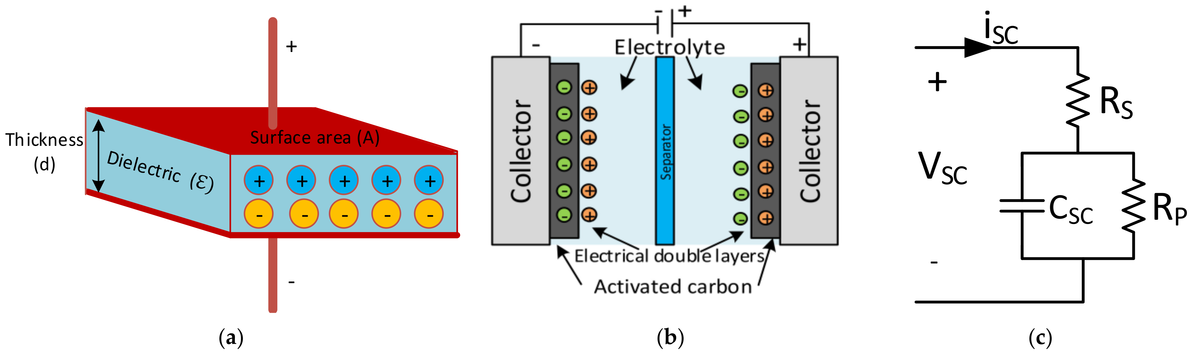
IJMS, Free Full-Text
Double layer (surface science) - Wikipedia
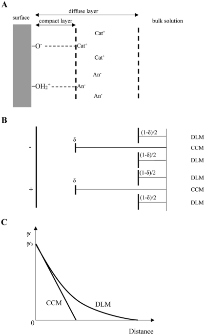
New structure of electrical double layer to modify triple-layer model at oxide–water interface

ars.els-cdn.com/content/image/3-s2.0-B978044459552

a) Structure of electric double layer, with the corresponding